Loading market data...
Tue, 20 Oct 2026
05:00:45 pm
Tue, 20 Oct 2026
05:00:45 pm

Rudransh Sangwan
Published at: July 16, 2026, 6:23 AM
Synopsis
The Union Cabinet has approved India Semiconductor Mission (ISM) 2.0 with a budgetary allocation of ₹1.27 lakh crore, marking one of the government's biggest investments in the country's semiconductor ecosystem. Alongside the mission, the Cabinet also approved a ₹62,500 crore Mobile Phone Manufacturing Scheme (MPMS) as part of a broader ₹2.19 lakh crore package of seven key policy decisions. The initiative aims to strengthen India's semiconductor design, fabrication, packaging, research, and talent ecosystem while positioning the country as a global electronics manufacturing hub.
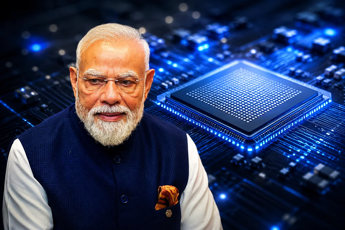
The Union Cabinet, chaired by Prime Minister Narendra Modi, has approved India Semiconductor Mission (ISM) 2.0 with a budgetary outlay of ₹1,27,500 crore, significantly expanding India's efforts to establish a globally competitive semiconductor manufacturing ecosystem. The approval builds upon the progress made under the first phase of the semiconductor mission and reflects the government's long-term strategy to reduce import dependence while strengthening domestic electronics manufacturing.
The Cabinet also cleared a ₹62,500 crore Mobile Phone Manufacturing Scheme (MPMS), reinforcing India's ambitions to become a leading global manufacturing destination for electronics and smartphones. Together, these initiatives form part of seven Cabinet decisions worth approximately ₹2.19 lakh crore, covering semiconductors, mobile manufacturing, railway infrastructure, urea policy, and urban infrastructure development.
Announcing the decisions after the Cabinet meeting, Union Minister for Electronics and Information Technology Ashwini Vaishnaw said that Semicon 2.0 represents the government's next phase of semiconductor development after the initial momentum generated under Semicon 1.0. The new programme focuses on creating capabilities across the complete semiconductor value chain, including chip design, fabrication, packaging, advanced research, equipment manufacturing, and skilled workforce development.
Semiconductors have become a strategic priority for governments worldwide due to their critical role in consumer electronics, automobiles, telecommunications, artificial intelligence, defence systems, industrial automation, healthcare devices, and data centres. Through ISM 2.0, India aims to strengthen supply chain resilience, attract global investments, and emerge as an important participant in the global semiconductor industry.
India Semiconductor Mission 2.0 has been structured as a comprehensive long-term programme that seeks to build an integrated semiconductor ecosystem rather than focusing only on chip fabrication. The initiative expands government support across manufacturing, design, research, packaging, materials, equipment, and talent development.
| Particular | Details |
|---|---|
| Programme | India Semiconductor Mission (ISM) 2.0 |
| Cabinet Approval Date | July 15, 2026 |
| Budget Allocation | ₹1,27,500 crore |
| Mobile Phone Manufacturing Scheme | ₹62,500 crore |
| Total Cabinet Package | Approximately ₹2.19 lakh crore |
| Objective | Build a complete semiconductor ecosystem in India |
| Focus Areas | Design, Fabrication, Packaging, R&D, Materials, Talent Development |
The semiconductor package represents one of the largest policy initiatives undertaken by the government to strengthen India's position within global electronics manufacturing and semiconductor supply chains.
The government has designed ISM 2.0 around six strategic pillars that collectively cover the semiconductor industry's entire value chain.
The first pillar focuses on strengthening India's semiconductor design capabilities by supporting domestic intellectual property (IP), chip architecture, and systems-on-chip (SoCs). Building on the success of Semicon 1.0, where over 100 startups entered semiconductor design, the government aims to position India as a global semiconductor design innovation hub.
The second pillar concentrates on semiconductor manufacturing equipment, specialty chemicals, gases, and raw materials. Developing domestic capabilities in these areas is expected to reduce dependence on imports while strengthening India's precision manufacturing ecosystem.
The third pillar seeks to attract more semiconductor fabrication facilities, including silicon fabs, compound semiconductor fabs, display fabs, and discrete component manufacturing units. The government expects India's first silicon fabrication plant to become operational by 2028.
The fourth pillar focuses on expanding India's Assembly, Testing, Marking and Packaging (ATMP) and Outsourced Semiconductor Assembly and Test (OSAT) ecosystem. As global companies diversify manufacturing locations, India aims to become an attractive destination for advanced semiconductor packaging operations.
The fifth pillar emphasizes research and development. The government plans to move beyond existing 28nm–110nm manufacturing technologies and invest in advanced semiconductor process technologies through collaborations with domestic and international research institutions.
The sixth pillar focuses on talent development by expanding semiconductor education and industry training programmes. More universities, engineering institutions, and industry partners are expected to participate in developing skilled manpower for chip design, fabrication, packaging, and clean-room operations.
| Six Strategic Pillars | Focus Area |
|---|---|
| Pillar 1 | Semiconductor Design & IP Development |
| Pillar 2 | Equipment, Materials & Chemicals |
| Pillar 3 | Semiconductor Fabrication (Fabs) |
| Pillar 4 | ATMP & OSAT Manufacturing |
| Pillar 5 | Research & Advanced Technologies |
| Pillar 6 | Talent Development & Skill Building |
The government highlighted that India Semiconductor Mission 2.0 builds on significant progress achieved under the first phase of the programme. Since the launch of Semicon 1.0, India has approved 12 semiconductor manufacturing projects involving cumulative investments exceeding ₹1.64 lakh crore.
These approved projects include one silicon fabrication facility, one silicon carbide fabrication unit, one integrated gallium nitride Micro LED display fabrication plant, and nine semiconductor packaging facilities. Several projects target strategic industries such as consumer electronics, automotive electronics, industrial automation, telecommunications, aerospace, and power electronics.
Commercial production has already commenced at manufacturing facilities established by Micron, Kaynes, and CG Semi, while another manufacturing unit is expected to begin operations during 2026.
On the semiconductor design side, the government has approved 24 startup and MSME design projects for financial assistance. Additionally, 105 startups and MSMEs have received access to Electronic Design Automation (EDA) software tools, enabling the development of semiconductor solutions for satellite communication, artificial intelligence, drones, IoT devices, smart meters, surveillance systems, telecom equipment, and LED drivers.
| Semicon 1.0 Progress | Status |
|---|---|
| Manufacturing Projects Approved | 12 |
| Total Approved Investment | Over ₹1.64 lakh crore |
| Silicon Fabs | 1 |
| Silicon Carbide Fab | 1 |
| Micro LED Display Fab | 1 |
| Semiconductor Packaging Units | 9 |
| Startups Using EDA Tools | 105 |
| Startup Design Projects Supported | 24 |
| Universities Training Students | 315 |
| Students Trained | Approximately 68,000 |
The approval of India Semiconductor Mission 2.0 significantly strengthens India's long-term industrial policy by encouraging investments across semiconductor manufacturing, electronics, and advanced technologies. The ₹1.27 lakh crore government allocation is expected to catalyse substantially higher private sector investment over the coming years as domestic and international companies establish manufacturing and design facilities in India.
The programme also complements the newly approved ₹62,500 crore Mobile Phone Manufacturing Scheme, which aims to deepen domestic value addition in smartphone manufacturing while reducing reliance on imported components. Together, the two schemes are expected to create stronger linkages between semiconductor production and electronics manufacturing, improving India's competitiveness within global supply chains.
| Business Area | Expected Impact |
|---|---|
| Semiconductor Manufacturing | Increased domestic capacity |
| Electronics Industry | Higher local value addition |
| Private Investment | Improved investment opportunities |
| Supply Chain | Reduced import dependence |
| Employment | Expansion of high-skilled jobs |
| Technology Development | Growth in semiconductor innovation |
The initiatives are also expected to generate opportunities for MSMEs, component manufacturers, engineering firms, research institutions, and technology startups participating in the broader semiconductor ecosystem.
India Semiconductor Mission 2.0 represents one of the country's most significant industrial policy initiatives in recent years. The programme is expected to support companies involved in semiconductor manufacturing, electronics, industrial automation, specialty chemicals, semiconductor equipment, engineering services, and chip design.
Listed companies operating across electronics manufacturing services (EMS), semiconductor packaging, industrial automation, specialty materials, and engineering solutions could potentially benefit from increased investment activity. However, the actual commercial impact will depend on project execution, private sector participation, technology partnerships, and global semiconductor demand.
The initiative also strengthens India's strategic position within global semiconductor supply chains at a time when countries worldwide are diversifying manufacturing away from concentrated production centres. Continued government support could improve India's attractiveness as an investment destination for multinational semiconductor companies.
| Stakeholder | Potential Impact |
|---|---|
| Semiconductor Companies | Higher investment opportunities |
| Electronics Manufacturers | Stronger domestic ecosystem |
| Startups | Increased funding and design support |
| Universities | Expanded semiconductor education |
| Investors | Long-term sector growth potential |
| Economy | Enhanced manufacturing competitiveness |
India Semiconductor Mission 2.0 marks a major step in the country's ambition to become a global semiconductor manufacturing and design hub. By expanding government support across the full semiconductor value chain, the programme aims to build long-term technological capabilities while reducing dependence on imported chips and strategic electronic components.
Going forward, investors and industry participants will closely monitor new project approvals, global semiconductor partnerships, fabrication facility announcements, and implementation timelines under the expanded programme. Progress in attracting leading global semiconductor manufacturers, advancing domestic research capabilities, and commercialising indigenous chip designs will be critical indicators of the mission's long-term success.
While semiconductor manufacturing requires substantial capital investment and long execution timelines, ISM 2.0 provides a comprehensive policy framework that could strengthen India's role in the global semiconductor industry over the coming decade.
India Semiconductor Mission 2.0 is the government's second-phase semiconductor development programme with a budget allocation of ₹1.27 lakh crore aimed at strengthening semiconductor design, fabrication, packaging, research, manufacturing equipment, and talent development across India.
The Union Cabinet has approved ₹1,27,500 crore for India Semiconductor Mission 2.0 and an additional ₹62,500 crore for the Mobile Phone Manufacturing Scheme, forming part of a broader ₹2.19 lakh crore package of Cabinet decisions.
The six pillars include semiconductor design, equipment and materials manufacturing, semiconductor fabrication, ATMP and OSAT packaging, research and development, and talent development through universities and industry collaboration.
Under the first phase, the government approved 12 semiconductor manufacturing projects with investments exceeding ₹1.64 lakh crore, supported 24 startup design projects, enabled 105 startups to access industry-standard EDA tools, and trained around 68,000 students across 315 universities.
The mission aims to reduce India's dependence on imported semiconductors, strengthen domestic manufacturing capabilities, attract global investment, create high-skilled employment, and position India as a key player in the global semiconductor supply chain.
Financial journalist specializing in market analysis, stock research, and investment trends. Dedicated to providing accurate, timely insights for informed decision-making.
Credentials: Experienced financial journalist with expertise in equity markets and economic analysis
The information provided in this article is for educational and informational purposes only and should not be construed as financial, investment, or legal advice. welomoney does not provide personalized investment recommendations.
For detailed terms and conditions, please read our Disclaimer and Terms of Service.

Diwali Muhurat Trading 2026 is scheduled for November 8 from 2:20 PM to 3:30 PM. See NSE and BSE timings, pre-open session and market schedule.

Sugar stocks fell up to 5.79% after the government barred sugarcane juice and syrup for FY27 ethanol procurement. Analysts flag earnings pressure.

NSE indices on October 16, 2026: Nifty IT rises 3.12%, Nifty 50 gains 0.49%, while Nifty FMCG, Capital Market and Bank indices decline.

India-US trade deal could influence Sensex, Nifty 50 and export stocks. Explore five sectors to watch and the key factors investors should track.

India agricultural growth may approach zero as El Niño threatens crops, with output potentially falling 4%.